- 您现在的位置:买卖IC网 > Sheet目录3881 > PIC18F8520T-E/PT (Microchip Technology)IC PIC MCU FLASH 16KX16 80TQFP
R01DS0060EJ0100 Rev.1.00
Page 140 of 168
Sep 13, 2011
RX630 Group
5. Electrical Characteristics
Note 1. The value in parentheses is used when ICMR3.NF[1:0] are set to 11b while a digital filter is enabled with ICFER.NFE = 1.
Note 2. Cb indicates the total capacity of the bus line.
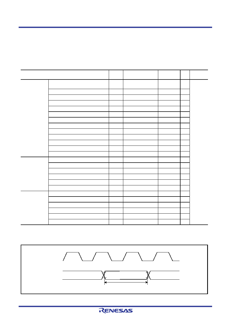
Figure 5.24
I/O Port Input Timing
Table 5.19
Timing of On-Chip Peripheral Modules (5)
Conditions: VCC = AVCC0 = VCC_USB = 2.7 to 3.6 V, VREFH/VREFH0 = 2.7 V to AVCC0
VSS = AVSS0 = VREFL/VREFL0 = VSS_USB = 0 V
PCLK = 8 to 50 MHz
Ta = Topr
High drive output is selected by the drive capacity control register.
Item
Symbol
Max.
Unit
Test
Conditions
RIIC
(Fast-mode+)
ICFER.FMPE = 1
SCL input cycle time
tSCL
8 (10) × (1/PCLK) +
240
—
ns
SCL input high pulse width
tSCLH
3 (5) × (1/PCLK) + 120
—
ns
SCL input low pulse width
tSCLL
5 × (1/PCLK) + 120
—
ns
SCL, SDA input rise time
tSr
—
120
ns
SCL, SDA input fall time
tSf
—
120
ns
SCL, SDA input spike pulse removal time
tSP
0
4 × (1/PCLK)
ns
SDA input bus free time
tBUF
5 × (1/PCLK) + 120
—
ns
Start condition input hold time
tSTAH
3 (5) × (1/PCLK) + 120
ns
Restart condition input setup time
tSTAS
5 × (1/PCLK) + 120
—
ns
Stop condition input setup time
tSTOS
3 (5) × (1/PCLK) + 120
—
ns
Data input setup time
tSDAS
50
—
ns
Data input hold time
tSDAH
0—
ns
SCL, SDA capacitive load
Cb
—
550
pF
Simple IIC
(Standard-mode)
SDA input rise time
tSr
—
1000
ns
SDA input fall time
tSf
—
300
ns
SDA input spike pulse removal time
tSP
0
4 × (1/PCLK)
ns
Data input setup time
tSDAS
250
—
ns
Data input hold time
tSDAH
0—
ns
SCL, SDA capacitive load
Cb
—
400
pF
Simple IIC
(Fast-mode)
SCL, SDA input rise time
tSr
20 + 0.1Cb
300
ns
SCL, SDA input fall time
tSf
20 + 0.1Cb
300
ns
SCL, SDA input spike pulse removal time
tSP
0
4 × (1/PCLK)
ns
Data input setup time
tSDAS
100
—
ns
Data input hold time
tSDAH
0—
ns
SCL, SDA capacitive load
Cb
—
400
pF
Port
PCLK
tPRW
发布紧急采购,3分钟左右您将得到回复。
相关PDF资料
XF2J-2624-11
CONN FPC 26POS 0.5MM SMT
PIC18F8585T-I/PT
IC PIC MCU FLASH 24KX16 80TQFP
XF2J-2424-11
CONN FPC 24POS 0.5MM SMT
PIC18LF6585T-I/PT
IC PIC MCU FLASH 24KX16 64TQFP
PIC18LF6680T-I/PT
IC PIC MCU FLASH 32KX16 64TQFP
XF2J-2224-11
CONN FPC 22POS 0.5MM SMT
PIC18F6525T-I/PT
IC PIC MCU FLASH 24KX16 64TQFP
PIC18F4439-E/ML
IC PIC MCU FLASH 6KX16 44QFN
相关代理商/技术参数
PIC18F8520T-I/PT
功能描述:8位微控制器 -MCU 32KB 2048 RAM 68I/O RoHS:否 制造商:Silicon Labs 核心:8051 处理器系列:C8051F39x 数据总线宽度:8 bit 最大时钟频率:50 MHz 程序存储器大小:16 KB 数据 RAM 大小:1 KB 片上 ADC:Yes 工作电源电压:1.8 V to 3.6 V 工作温度范围:- 40 C to + 105 C 封装 / 箱体:QFN-20 安装风格:SMD/SMT
PIC18F8520T-I/PTG
功能描述:8位微控制器 -MCU 32KB 2048 RAM 68I/O Lead Free Package RoHS:否 制造商:Silicon Labs 核心:8051 处理器系列:C8051F39x 数据总线宽度:8 bit 最大时钟频率:50 MHz 程序存储器大小:16 KB 数据 RAM 大小:1 KB 片上 ADC:Yes 工作电源电压:1.8 V to 3.6 V 工作温度范围:- 40 C to + 105 C 封装 / 箱体:QFN-20 安装风格:SMD/SMT
PIC18F8525-E/PT
功能描述:8位微控制器 -MCU 48KB 3840 RAM 68I/O RoHS:否 制造商:Silicon Labs 核心:8051 处理器系列:C8051F39x 数据总线宽度:8 bit 最大时钟频率:50 MHz 程序存储器大小:16 KB 数据 RAM 大小:1 KB 片上 ADC:Yes 工作电源电压:1.8 V to 3.6 V 工作温度范围:- 40 C to + 105 C 封装 / 箱体:QFN-20 安装风格:SMD/SMT
PIC18F8525-I/PT
功能描述:8位微控制器 -MCU 48KB 3840 RAM 68I/O RoHS:否 制造商:Silicon Labs 核心:8051 处理器系列:C8051F39x 数据总线宽度:8 bit 最大时钟频率:50 MHz 程序存储器大小:16 KB 数据 RAM 大小:1 KB 片上 ADC:Yes 工作电源电压:1.8 V to 3.6 V 工作温度范围:- 40 C to + 105 C 封装 / 箱体:QFN-20 安装风格:SMD/SMT
PIC18F8525T-I/PT
功能描述:8位微控制器 -MCU 48KB 3840 RAM 68I/O RoHS:否 制造商:Silicon Labs 核心:8051 处理器系列:C8051F39x 数据总线宽度:8 bit 最大时钟频率:50 MHz 程序存储器大小:16 KB 数据 RAM 大小:1 KB 片上 ADC:Yes 工作电源电压:1.8 V to 3.6 V 工作温度范围:- 40 C to + 105 C 封装 / 箱体:QFN-20 安装风格:SMD/SMT
PIC18F8527-I/PT
功能描述:8位微控制器 -MCU 48 KB 4K RAM 70 I/O RoHS:否 制造商:Silicon Labs 核心:8051 处理器系列:C8051F39x 数据总线宽度:8 bit 最大时钟频率:50 MHz 程序存储器大小:16 KB 数据 RAM 大小:1 KB 片上 ADC:Yes 工作电源电压:1.8 V to 3.6 V 工作温度范围:- 40 C to + 105 C 封装 / 箱体:QFN-20 安装风格:SMD/SMT
PIC18F8527T-I/PT
功能描述:8位微控制器 -MCU 48 KB 4K RAM 70 I/O RoHS:否 制造商:Silicon Labs 核心:8051 处理器系列:C8051F39x 数据总线宽度:8 bit 最大时钟频率:50 MHz 程序存储器大小:16 KB 数据 RAM 大小:1 KB 片上 ADC:Yes 工作电源电压:1.8 V to 3.6 V 工作温度范围:- 40 C to + 105 C 封装 / 箱体:QFN-20 安装风格:SMD/SMT
PIC18F8585-E/PT
功能描述:8位微控制器 -MCU 48KB 3328 RAM 68I/O RoHS:否 制造商:Silicon Labs 核心:8051 处理器系列:C8051F39x 数据总线宽度:8 bit 最大时钟频率:50 MHz 程序存储器大小:16 KB 数据 RAM 大小:1 KB 片上 ADC:Yes 工作电源电压:1.8 V to 3.6 V 工作温度范围:- 40 C to + 105 C 封装 / 箱体:QFN-20 安装风格:SMD/SMT